
Wafer Economics in the Age of Agents: Why TSMC’s Sixth Consecutive Record Quarter Changes the Math for Every AI Lab
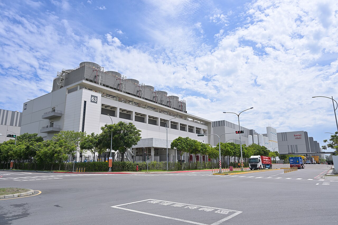
On October 15, 2026, Taiwan Semiconductor Manufacturing Company reported third-quarter results that did more than beat estimates. They quantified, in hard dollars and process nodes, the structural reordering of the global computing stack. Consolidated revenue reached NT$1,494.24 billion, or roughly $46.72 billion in U.S. dollars—up 50.9 percent year-over-year and 17.6 percent sequentially. Net income surged 68.7 percent to NT$763.06 billion, or about $23.7 billion, marking the sixth consecutive quarter of record profits. Diluted earnings per share hit NT$29.43, or $4.60 per ADR. Gross margin held at 66.4 percent, operating margin at 58.7 percent, and net profit margin at 51.1 percent. Advanced technologies defined as 7-nanometer and below accounted for 79 percent of wafer revenue. Within that, the still-ramping 2-nanometer node already contributed 8 percent, up from 3 percent the prior quarter, while 3-nanometer led at 33 percent.
These figures, drawn directly from TSMC’s own release and management commentary, arrive at a moment when agentic AI systems are moving from demonstration to daily operation. The same week Meta published the weights of Muse Spark Open, an 816-billion-parameter mixture-of-experts model optimized for long-horizon coding and multi-step reasoning. That release, and the broader wave of open and closed models demanding sustained inference and continuous training, does not merely consume chips. It multiplies the economic value of every advanced wafer that leaves a TSMC fab. The quarter’s numbers therefore function less as a traditional earnings beat and more as a public accounting of who controls the physical substrate on which the next generation of autonomous digital labor will be built.
The Numbers Behind the Node Shift
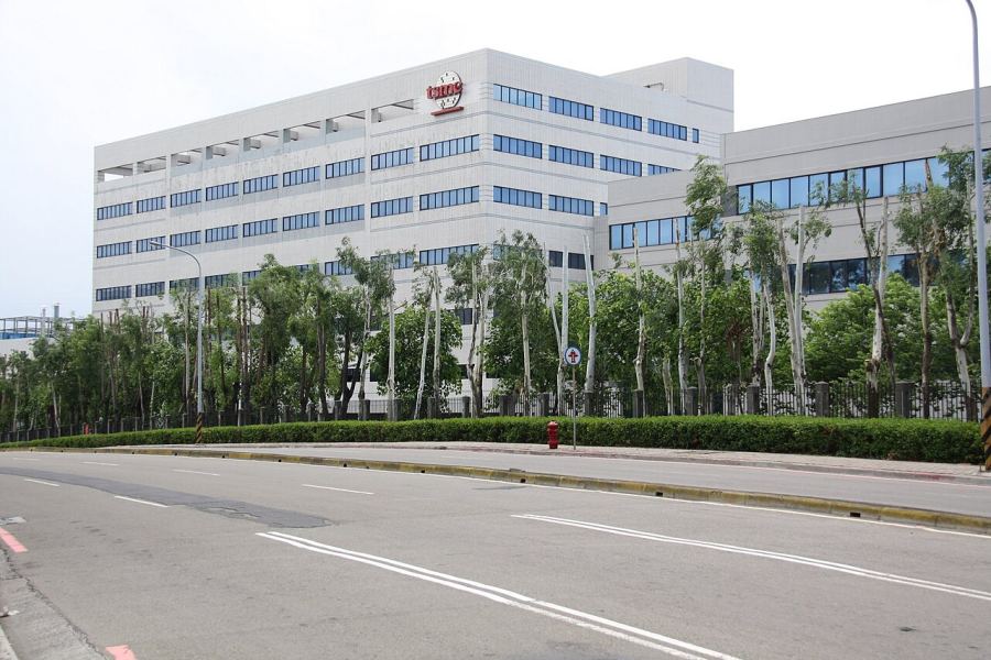
TSMC’s breakdown by technology and by platform makes the concentration explicit. High-performance computing, the category that encompasses AI accelerators, networking silicon, and the CPUs that orchestrate them, represented 68 percent of net revenue. Smartphones accounted for 21 percent. Sequentially, HPC revenue rose 22 percent. Management guided fourth-quarter revenue between $52.3 billion and $54.3 billion, implying further acceleration into year-end, and raised the full-year 2026 U.S.-dollar revenue growth outlook to approximately 44 percent. Capital expenditure for the 2026–2028 period is expected to rise substantially relative to the prior three-year span, consistent with the company’s already announced multi-hundred-billion-dollar U.S. commitment centered on Arizona.
The 2-nanometer contribution of 8 percent is particularly telling. That node is still early in its volume ramp, yet it is already material. TSMC has stated that 2-nanometer family capacity in 2027 will more than double relative to earlier plans. For AI labs designing custom accelerators or relying on merchant GPUs, this ramp determines both the availability of the densest transistors and the cost trajectory of inference. The gross-margin resilience at 66.4 percent, only modestly diluted by the 2-nanometer introduction, indicates that pricing power remains intact even as volumes scale.
Independent reporting from Reuters, CNBC, and others confirmed the beat against consensus and the sixth-straight record. What the official release adds is the precise mix: 3-nanometer at 33 percent, 5-nanometer at 28 percent, 7-nanometer at 10 percent. This is not a commodity foundry cycle. It is a foundry whose leading-edge share of revenue continues to expand while absolute volumes at those nodes set new records. For the internal TechMash analysis of memory-density claims and market reactions, see The 4F² Shockwave.
Why the Quarter Rewrites Lab Economics
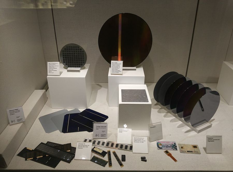
The economic implication for AI laboratories is straightforward yet under-appreciated in pure model-benchmark discussions. Every incremental improvement in model capability that increases inference tokens, agent steps, or training compute must ultimately clear the same physical constraint: the number of advanced wafers TSMC can ship. When an open-weight model such as Muse Spark Open is released with a 1-million-token context and native multimodal perception, the downstream effect is not only developer adoption but also increased demand for the silicon that runs those workloads at acceptable latency and cost. Meta’s earlier Muse Wonder release, analyzed in Meta’s Muse Wonder Resets the Agent Race, already demonstrated that long-horizon memory and focus features drive sustained compute.
This dynamic also reframes the competitive position of pure-play labs versus hyperscalers that can co-design silicon. Apple, Nvidia, Broadcom, Google, Amazon, Microsoft, Meta, and OpenAI are all customers competing for the same leading-edge capacity. The Arizona expansion is the company’s response to that demand and to geopolitical diversification pressures. Yet even with that capital deployment, management has described demand as continuing to outstrip supply.
For labs that cannot secure preferential allocation, the practical consequence is higher effective cost of inference or delayed deployment of agentic features. The same constraint appears in adjacent domains. Google’s Project Suncatcher orbital TPU experiment, covered in A Kilowatt in Orbit and its precursor Orbiting the AI Bottleneck, tests extreme environments precisely because ground-based power and cooling limits are already binding.
What to Watch Through 2027

Several near-term indicators will reveal whether the current trajectory holds or encounters friction. First is the pace of the 2-nanometer ramp. Second is the realization of the raised capital-expenditure plans and the Arizona timeline. High-volume production on N4 is already underway in the first Arizona fab; subsequent phases target N3 and then N2-class technologies. Packaging capacity, particularly CoWoS and related interposer supply, remains a parallel bottleneck.
Third is the evolution of agentic workload characteristics. As models move from chat to persistent agents that call tools, maintain memory, and operate across multimodal inputs, the ratio of inference to training compute is expected to rise. Macroeconomic caution for 2027, which management has flagged, centers on broader uncertainty rather than a slowdown in AI-specific demand. The company continues to describe AI-related orders as robust and extending into networking and agentic CPUs.
Finally, competitive responses matter. Chinese foundries and memory makers continue to advance mature and intermediate nodes, and density claims in DRAM have already produced market volatility. Those developments can affect overall system cost, yet they do not currently substitute for the leading-edge logic that defines the highest-performance accelerators. The consumer-side growth of Meta’s Muse agent, previously tracked in Beyond the Chatbot Hype, already illustrated demand for background task completion.
Conclusion: Substrate as Strategy
TSMC’s third-quarter 2026 results do not merely confirm that AI demand remains strong. They demonstrate that the economic returns to leading-edge process technology have become self-reinforcing at a scale previously associated only with the largest software platforms. A 51.1 percent net margin on nearly $47 billion of quarterly revenue, achieved while ramping a new node and funding multi-year capacity expansions, is the financial expression of a technological bottleneck that no single lab can internalize. Every organization building or deploying agentic systems—whether through closed frontier models, open weights, or custom silicon—is ultimately negotiating for a share of the same wafer output.
The practical consequence is that process-node roadmaps, packaging capacity, and geographic diversification now sit alongside model architecture and data strategy as first-order variables. Labs that treat silicon supply as an external commodity will face higher costs and longer lead times as agentic workloads scale. Those that integrate foundry relationships, co-design, or efficiency innovations will capture a larger share of the value created by each incremental improvement in model capability. The sixth consecutive record quarter is therefore less a peak than a baseline. It establishes the financial and physical foundation on which the next several years of AI deployment will be constructed.
External reference: TSMC Reports Third Quarter EPS of NT$29.43 and the accompanying management materials. Additional market context appears in contemporaneous reporting from Reuters and CNBC, which independently confirmed the record and the guidance.
Comments
0